
Master Of Packets
New elf
- Joined
- Oct 11, 2025
- Messages
- 3
United States Testers only, please ( don't think I could afford the shipping  . Unless you would like to pay for shipping.
Long-time lurker, first time posting about something I built.
**It started with boards that kept dying.**
We all know how this goes. Something gets wired wrong at eleven at night, a run gets pinched, a supply gets swapped in a hurry — and a board that had no business dying takes a whole prop dark for the rest of the evening. I wanted hardware that shrugs off the bad-judgment moments instead of turning them into a repair job in the driveway.
So I taught myself PCB design and built the board I wanted to own — one where every failure mode has a specific part standing in front of it, chosen from a datasheet and verified against the copper.
Background, so you know where I'm coming from: day job is senior network architect — infrastructure that isn't allowed to fail. Nights and weekends it's a bench, a soldering iron, and pixels I keep pushing past what the hardware was meant to do. The discipline comes from the day job. The lights are where I get to have fun with it.
**What it is**
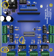
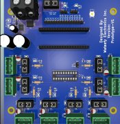
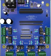
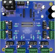
The NODE family — three boards, one protected 8-port pixel stage underneath all of them. Three isolated power domains, a fuse on every single output, non-destructive reverse-polarity protection, 5–48 V with no jumpers to change input voltage, 30 A at standard copper, runs stock WLED. Nothing in the power path runs near its limit. What changes between the three is the brain on top and how it gets on the network.
**NODE Mini** — Seeed XIAO ESP32-S3, Wi-Fi. Compact, standard runs, get it on the network and drive pixels.
**NODE Flex** — universal DevKit carrier. Both 0.9″ and 1.0″ row spacings on the board, jumper-mapped to the outputs. Seat whatever ESP32 you already have; swap it when that one goes EOL, so the compatibility list can't go stale. (Olimex and LilyGo use odd row spacing and won't drop straight in — everything else I've tried does.)
**NODE Backbone** — Waveshare ESP32-S3-ETH-POE with a dedicated W5500. Wired 10/100 and PoE for the install that outgrew Wi-Fi. Deterministic frame timing, one cable for power and control to the node.
Design priorities, briefly: protection first — assume it gets abused. Honest specs — real ratings, real derating, trade-offs stated out loud, no spec-sheet trophies that fall apart when someone does the math. Serviceable — fuses you swap by hand, socketed parts, a board meant to be fixed and kept running rather than thrown out when one channel dies. Open — WLED out of the box, docs and board definitions on GitHub.
I'll say plainly that the Bong69 and the QuinLED-Dig-Quad were both inspirations here. I've run them, I like them, and seeing what they did well is a good part of why I thought I could take a swing at my own. This isn't me trying to one-up anybody — it's my take on the same problem, with different priorities in a few places.
**Why I'm posting**
I want people who will actually work it hard and tell me what's wrong. Not looking for a pat on the back — looking for the thing I didn't think of. I've got a handful of boards from the first run and I'll send them out free. No cost, no shipping, no strings, no video required, no NDA.
What I'm hoping for in return is an honest read. Load it up, run a real prop on it, push the channel count, tell me where it flinches. If it turns out my board is worse than what you're already running, I'd rather hear that from you now than after somebody's paid for one (If I decide to try and sell them).
There's no team here to hide behind. If something's wrong with it, it's on me, and I'll make it right.
**What makes someone a good fit**
- Running a show at real scale, or you'll load these channels properly on the bench
- Comfortable in WLED and xLights, and can tell a firmware problem from a hardware one
- You'll actually report back — good, bad, or "this is fine but here's what annoyed me"
- Bonus: you run a Bong69 or a QuinLED-Dig-Quad and can compare directly. I want to know where mine falls short.
**Where things stand**
Stock is thin — this is a small validation run and I'm counting boards on one hand. The test units are free and separate from anything else. I'm looking for people who'll find the problems in this one.
And plainly: this is V1. It works, I've run it, but first-article hardware is first-article hardware. That's the whole reason I want it in the hands of people who'll push it.
I've got full datasheets — power architecture, derating tables against input voltage, and a section on where the Bong69 and QuinLED are the better choice, because in a few real ways they are. Happy to post or link them if there's interest.
Reply here or PM me. And if you want to get into the weeds on the design, I'm happy to — that's the fun part.
Thanks,
John — Wateefy Electronics
github.com/johnvoipguy
. Unless you would like to pay for shipping.Long-time lurker, first time posting about something I built.
**It started with boards that kept dying.**
We all know how this goes. Something gets wired wrong at eleven at night, a run gets pinched, a supply gets swapped in a hurry — and a board that had no business dying takes a whole prop dark for the rest of the evening. I wanted hardware that shrugs off the bad-judgment moments instead of turning them into a repair job in the driveway.
So I taught myself PCB design and built the board I wanted to own — one where every failure mode has a specific part standing in front of it, chosen from a datasheet and verified against the copper.
Background, so you know where I'm coming from: day job is senior network architect — infrastructure that isn't allowed to fail. Nights and weekends it's a bench, a soldering iron, and pixels I keep pushing past what the hardware was meant to do. The discipline comes from the day job. The lights are where I get to have fun with it.
**What it is**
The NODE family — three boards, one protected 8-port pixel stage underneath all of them. Three isolated power domains, a fuse on every single output, non-destructive reverse-polarity protection, 5–48 V with no jumpers to change input voltage, 30 A at standard copper, runs stock WLED. Nothing in the power path runs near its limit. What changes between the three is the brain on top and how it gets on the network.
**NODE Mini** — Seeed XIAO ESP32-S3, Wi-Fi. Compact, standard runs, get it on the network and drive pixels.
**NODE Flex** — universal DevKit carrier. Both 0.9″ and 1.0″ row spacings on the board, jumper-mapped to the outputs. Seat whatever ESP32 you already have; swap it when that one goes EOL, so the compatibility list can't go stale. (Olimex and LilyGo use odd row spacing and won't drop straight in — everything else I've tried does.)
**NODE Backbone** — Waveshare ESP32-S3-ETH-POE with a dedicated W5500. Wired 10/100 and PoE for the install that outgrew Wi-Fi. Deterministic frame timing, one cable for power and control to the node.
Design priorities, briefly: protection first — assume it gets abused. Honest specs — real ratings, real derating, trade-offs stated out loud, no spec-sheet trophies that fall apart when someone does the math. Serviceable — fuses you swap by hand, socketed parts, a board meant to be fixed and kept running rather than thrown out when one channel dies. Open — WLED out of the box, docs and board definitions on GitHub.
I'll say plainly that the Bong69 and the QuinLED-Dig-Quad were both inspirations here. I've run them, I like them, and seeing what they did well is a good part of why I thought I could take a swing at my own. This isn't me trying to one-up anybody — it's my take on the same problem, with different priorities in a few places.
**Why I'm posting**
I want people who will actually work it hard and tell me what's wrong. Not looking for a pat on the back — looking for the thing I didn't think of. I've got a handful of boards from the first run and I'll send them out free. No cost, no shipping, no strings, no video required, no NDA.
What I'm hoping for in return is an honest read. Load it up, run a real prop on it, push the channel count, tell me where it flinches. If it turns out my board is worse than what you're already running, I'd rather hear that from you now than after somebody's paid for one (If I decide to try and sell them).
There's no team here to hide behind. If something's wrong with it, it's on me, and I'll make it right.
**What makes someone a good fit**
- Running a show at real scale, or you'll load these channels properly on the bench
- Comfortable in WLED and xLights, and can tell a firmware problem from a hardware one
- You'll actually report back — good, bad, or "this is fine but here's what annoyed me"
- Bonus: you run a Bong69 or a QuinLED-Dig-Quad and can compare directly. I want to know where mine falls short.
**Where things stand**
Stock is thin — this is a small validation run and I'm counting boards on one hand. The test units are free and separate from anything else. I'm looking for people who'll find the problems in this one.
And plainly: this is V1. It works, I've run it, but first-article hardware is first-article hardware. That's the whole reason I want it in the hands of people who'll push it.
I've got full datasheets — power architecture, derating tables against input voltage, and a section on where the Bong69 and QuinLED are the better choice, because in a few real ways they are. Happy to post or link them if there's interest.
Reply here or PM me. And if you want to get into the weeds on the design, I'm happy to — that's the fun part.
Thanks,
John — Wateefy Electronics
github.com/johnvoipguy

 You say "it's my take on the same problem, with different priorities in a few places" but what are the priorities? Why would someone use this over the current boards?